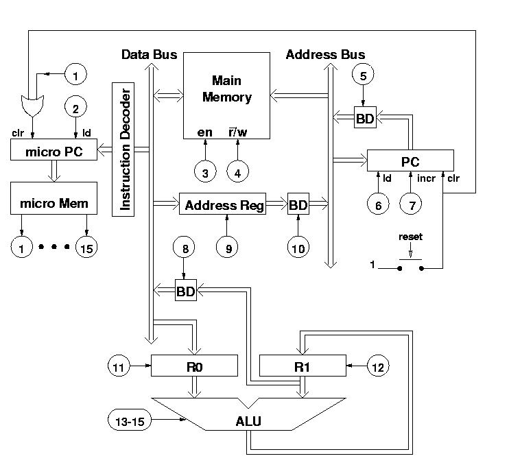

To the left in the diagram, you find the micro memory containing up to 64 different addresses each with 15 bits (numbered 1 to 15) that we call the micro operations or MOPs for short. The MOPs control every aspect of the computer.
To the left, you also find the micro PC, which is a counter register with clear. The width of the micro PC is 6 bits for a total of 64 different values. The micro PC is controlled by MOPs number 1 and 2. When MOP number 1 has the value 1, the micro PC will be cleared after the next clock pulse. Similarly, MOP number 2 will cause a new value to be loaded into the micro PC from the instruction decoder. The micro PC can also be cleared manually from the reset button. Since the clr input of the micro PC takes priority over the ld input, this will always happen when the reset button is pressed, independently of the value of MOP number 2.
The final item to the left of the data bus is the instruction decoder. Its job is to translate instruction codes to addresses in the micro memory where the micro program for the instruction starts. The input to the instruction decoder is the low 5 bits of the data bus, and the output is 6 bits wide.
The lower part of the diagram is the arithmetic unit with two general-purpose registers, R0 and R1. Whether R0 is loaded from the data bus is determined by MOP number 11. Whether R1 is loaded from the output of the ALU is controlled by MOP number 12. The ALU uses MOPS 13 to 15 to control what operation is to be performed. The inputs (8 bits wide) are taken from the registers R0 and R1 and the output (also 8 bits wide for now) goes to the input of R1. The output of R1 can be connected to the data bus by MOP number 8 which is connected to a bus driver (BD) which in effect closes the connection from the output of R1 to the data bus.
The upper middle part is the main memory. The enable input is conrolled by MOP number 3, and its r/w input is controlled by MOP number 4. When MOP number 4 has the value 1, the memory is written. The address of the memory is taken from the address bus and that date is output to the data bus (in the case of read) or taken from the data bus (in the case of write). Thus the data lines of the memory are bidirectional.
In the middle of the diagram, you find another register called the address register. It is used to communicate data from the data bus to the address bus. It is loaded whenever MOP number 9 has the value 1. The contents of the address register can be communicated to the address bus through a bus driver conrolled by MOP number 10. This way, data from main memory or from R1 can be used as addresses in main memory.
To the right of the diagram, you find the program counter (or PC) in the form of a counter register with clear and explicit increment. The clr signal takes priority so that the reset button always works. If the clr signal is 0 but the ld signal (MOP 6) is 1, then PC is loaded from the address bus. If clr and ld are 0 but incr (MOP 7) is 1, PC is incremented after the next clock pulse. Finally, if clr, ld and incr are all 0, then PC retains its value after the clock pulse. The value of PC can be communicated to the data bus through a bus driver by MOP number 5. This is the way instructions are fetched for execution.
000000: 011010100000000 (fetch)As you can see, MOPs number 2, 3, 5, and 7 have the value 1, and all others have the value 0.
00000: 000001 (NOP)The micro program for NOP does nothing, so all we have to do is make sure that after its execution, the contenst of micro PC is 0, so that the next instruction is loaded. Every micro program for instructions will be terminated by setting MOP number 1 to 1 for exactly this reason. With the micro program for NOP, where is the contents so far of the micro memory
000000: 011010100000000 (fetch)
000001: 100000000000000 (NOP)
The opcode for LDIMM will be 1 (the first free opcode), and the start of the micro program for LDIMM will be on address 2 in the micro memory (the first available address). Our instruction decoder now looks like this:
00000: 000001 (NOP)
00001: 000010 (LDIMM)
To implement the LDIMM instruction we shall need to address the main memory using the contents of PC. PC already contains the address of the argument, since the instruction fetch program incremented PC after fetching and decoding the instruction code. For that purpose, we use MOP number 5. We also need to read from main memory using MOP number 3 and store the value read into R0 using MOP number 11. By convention, we also increment PC so that it points to the instruction code of the next instruction. All of this can be done in one clock cycle, so in the next clock cycle, we need to fetch the next instruction. To make that happen, we set MOP number 1 to 1. We now have the following contents of the micro memory:
000000: 011010100000000 (fetch)
000001: 100000000000000 (NOP)
000010: 101010100010000 (LDIMM)
The first available instruction code is 2 and the first available address in micro memory is 3, so we now have the following contents of the instruction decoder:
00000: 000001 (NOP)
00001: 000010 (LDIMM)
00010: 000011 (LD)
The plan for implementing LD is as follows: First use the contents of PC to address memory (MOPs 5 and 3), and load the contents into the address register (using MOP number 9). Simultaneously, increment PC (MOP 7). Then, in the next cycle, use the address register to address memory (MOPs 10 and 3)) and load the contents into R0 (MOP 11). As you can see, this instruction requires two cycles, simply because two different addresses and contents of main memory need to be used, and that we have only one address bus and one data bus. By convention, we increment PC as soon as possible (after the first cycle). Here is the contents of micro memory so far:
000000: 011010100000000 (fetch)
000001: 100000000000000 (NOP)
000010: 101010100010000 (LDIMM)
000011: 001010101000000 (LD)
000011: 101000000110000 (LD)
As usual we pick the first available opcode and address in micro memory giving the following contents of the instruction decoder so far:
00000: 000001 (NOP)
00001: 000010 (LDIMM)
00010: 000011 (LD)
00011: 000101 (ST)
To implement the ST instruction, we have to be a bit more careful that we have been so far. The reason is that the memory is not synchronous. We must make sure that the values on the data bus and address bus are stable before we attempt to write into memory. The only way we can make sure this is the case is to separate them into different clock cycles. We also have to make sure the memory gets the write signal (MOP 4) before the enable signal (MOP 3). Otherwise, there is a risk that that the memory is read for a brief moment, which gives conflicting values on the data bus with possible circuit destruction as a result.
This is thus the plan for the ST instruction: in the first cycle, load the argument of the instruction (indicating the address to store into) into the address register, just as with the LD instruction. In the next cycle, use MOPs 8 and 10 to get the data bus and address bus stable. In the next cycle, add the write signal (MOP 4). In the next cycle, add the enable signal (MOP 3). Then in the next signal, remove the enable signal, but keep all the others (otherwise, again we may have the same problems). In the next and final cycle, remove the write signal, but keep the others. Here is the complete contents of micro memory so far:
000000: 011010100000000 (fetch)
000001: 100000000000000 (NOP)
000010: 101010100010000 (LDIMM)
000011: 001010101000000 (LD)
000100: 101000000110000 (LD)
000101: 001010101000000 (ST)
000110: 000000010100000 (ST)
000111: 000100010100000 (ST)
001000: 001100010100000 (ST)
001001: 000100010100000 (ST)
001010: 100000010100000 (ST)
00000: 000001 (NOP)
00001: 000010 (LDIMM)
00010: 000011 (LD)
00011: 000101 (ST)
00100: 001011 (COPY)
00101: 001100 (SHL)
00110: 001101 (SHR)
00111: 001110 (ADD)
01000: 001111 (SUB)
01001: 010000 (AND)
01010: 010001 (OR)
01011: 010010 (NOT)
The implementation of each of thes instruction consists simply of emitting the right values of MOPs 13, 14, and 15, and of emitting MOP number 12 to make sure the resulting value is stored in R1. Here is the contents of the micro memory so far:
000000: 011010100000000 (fetch)
000001: 100000000000000 (NOP)
000010: 101010100010000 (LDIMM)
000011: 001010101000000 (LD)
000100: 101000000110000 (LD)
000101: 001010101000000 (ST)
000110: 000000010100000 (ST)
000111: 000100010100000 (ST)
001000: 001100010100000 (ST)
001001: 000100010100000 (ST)
001010: 100000010100000 (ST)
001011: 100000000001000 (COPY)
001100: 100000000001001 (SHL)
001101: 100000000001010 (SHR)
001110: 100000000001011 (ADD)
001111: 100000000001100 (SUB)
010000: 100000000001101 (AND)
010001: 100000000001110 (OR)
010010: 100000000001111 (NOT)
As usual, we pick the first available opcode and address in micro memory, giving the following contents of the instruction decoder so far:
00000: 000001 (NOP)
00001: 000010 (LDIMM)
00010: 000011 (LD)
00011: 000101 (ST)
00100: 001011 (COPY)
00101: 001100 (SHL)
00110: 001101 (SHR)
00111: 001110 (ADD)
01000: 001111 (SUB)
01001: 010000 (AND)
01010: 010001 (OR)
01011: 010010 (NOT)
01100: 010011 (JAL)
The JAL instruction has one argument, the address to jump to. The plan for implementing the JAL instruction is as follows: In the first cycle, load the argument into the address register as will LD and ST. In the next cycle, use MOPs 10 and 6 to store this value into PC. While it is not strictly necessary to increment PC in the first cycle since it is going to be altered anyway in the second cycle, we do it anyway for consistency. Here is the contents of micro memory so far:
000000: 011010100000000 (fetch)
000001: 100000000000000 (NOP)
000010: 101010100010000 (LDIMM)
000011: 001010101000000 (LD)
000100: 101000000110000 (LD)
000101: 001010101000000 (ST)
000110: 000000010100000 (ST)
000111: 000100010100000 (ST)
001000: 001100010100000 (ST)
001001: 000100010100000 (ST)
001010: 100000010100000 (ST)
001011: 100000000001000 (COPY)
001100: 100000000001001 (SHL)
001101: 100000000001010 (SHR)
001110: 100000000001011 (ADD)
001111: 100000000001100 (SUB)
010000: 100000000001101 (AND)
010001: 100000000001110 (OR)
010010: 100000000001111 (NOT)
010011: 001010101000000 (JAL)
010100: 100001000100000 (JAL)